My third FPGA (for 10€)
Sipeed Tang Nano FPGA development board
I like FPGA development boards and I’m excited that there are products that exist outside of the Xilinx / Intel duopoly. This branch of the Chinese semiconductor industry is still developing and I was curious enough to order the Sipeed Tang Nano development board.
This article describes my experience after experimenting with the board and the development tools from the vendor.
It comes in a small and breadboard-friendly package measuring 58x21 mm, the shape reminds me of Arduino Nano.
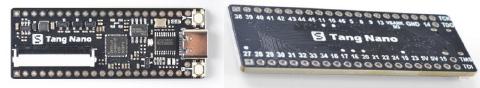
Sipeed Tang Nano board
The onboard FPGA chip is GOWIN GW1N-LV1QN48C6/I5, based on 55 nm procss, equipped with 1152 LUT4 logic resources, 1 PLL and 4 Block RAM (72 kbit total). The onboard crystal ticks at 24 MHz. USB-C connector is a welcome sight, it serves both as a power and programming interface. I counted 29 pins available to the user, which should be fine for little projects.
The development board also features a 40-pin connector for the 800x480 LCD display , the display itself is available separately for around $25 including shipping. I didn’t get the display to save some money as I have plenty of displays around.
As for the There’s also 64 Mbit PSRAM, I’m not really sure how to use it as I could not find any documentation on it. The lack of any hardware multiplier could pose a problem for some projects.
1152 LUTs offers definitely less capacity compared to the smallest Xilinx / Intel chips, which provide around 6000 logic cells. However, it should be sufficient for small glue logic / adapter kind of projects.
The documentation
There’s an official website that offers a walkthrough with two sample projects and is curiously missing the last one dealing with the onboard PSRAM. I wasn’t much impressed by the official docs as they skipped a few steps that could confuse a beginner (me). There’s a nice pinout schematic available.
I was much happier with a series of articles by Dave Vanden Bout at xess.com , which contained a nice getting started tutorial and a very valuable pinout spreadsheet .
The tools
The first project I built was the traditional ‘blinky’ - blinking the built-in RGB LED in different colors.
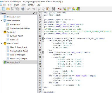
The tool of choice is
The tool supports both Verilog and VHDL, it includes all basic tools such as schematic viewer, IP core generator and a floor planner.
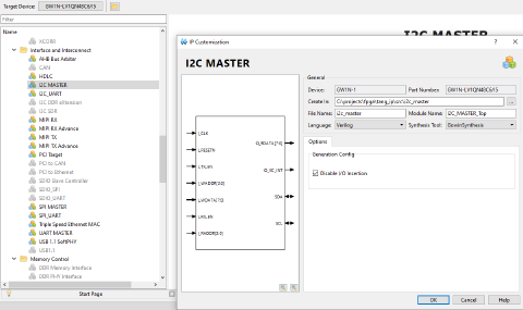
There are also several IP cores available for things such as I2C, MIPI, SPI and curiously enough also USB SoftPHY core.
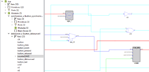
Schematic viewer - we can view individual modules, highlight nets and jump to source from individual primitives
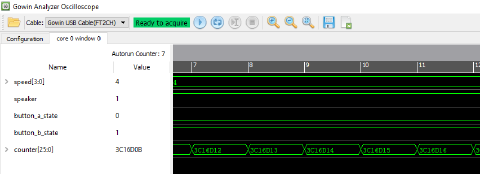
There’s also Gowin Analyzer Oscilloscope that allows you to capture signals based on a user-defined trigger, store them in the internal memory and stream the results to the PC, similar to SignalTap logic analyzer from Intel.
Open-source?
It would have been cool if the Chinese vendors embraced the open source toolchain such as Symbiflow / yosys / nextpnr. There’s a project Apicula that aims to document the GOWIN bitstream and make it usable with the open source tools.
A slightly more advanced project
I built a metronome by wiring a buzzer to the board. You can control the tempo with two built-in pushbuttons. I wanted to make the tempo slower or faster with two buttons and also change the LED pattern on each beat.
Because I only had an active 3 kHz buzzer on hand, I produced a tick by pulsing it for 2.5 ms. A debouncer and synchronizer module instance was required for each button. A speed generator module implemented a look up table that converted a “speed” selection to a number of clock cycles. The top module contained wiring between the modules and the ticking logic itself.
Verilog sources can be found on GitHub .
I’m aware that this kind of project is easier to implement on a microcontroller, but this was also fun.
This is how it looks in action:
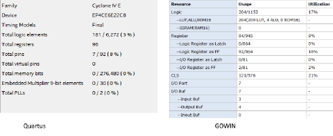
GOWIN vs Quartus resource usage
I ported the metronome design to Altera Cyclone IV using Quartus, as I was mostly interested in the efficiency of the synthesizer and wanted to compare the resulting resource usage. Both the GW1N-LV1QN48C6/I5 and EP4CE6E22C8 feature 4-LUT architecture, so the usage should be roughly the same.
Afte running the synthesis Quartus used 181 logic elements vs 204 used by GOWIN, which is a difference of 12%.
Synthesis speed
Producing the bitstream (synthesize, place & route, etc) of this sample design takes 5.5 seconds in GOWIN compared to 53 seconds on my machine, which is faster by an order of magnitude. I suspect that Quartus scales better once one graduates from toy projects to a sizable ones.
Pros and cons
+ Really fast synthesis for simple projects
+ Simple development environment
+ HTML reports
+ USB-C connector
- The license acquisition process
- Very modest hardware resources, no hardware multipliers, only one PLL
- Documentation is worse compared to competition
- Much weaker community support compared to competition
Do I recommend it?
Y…es. When I was starting out I was happier with a Xilinx/Altera development board with more peripherals, such as built-in buttons, 7-segment displays, LEDs and a VGA port as I’m a bit reluctant to solder or build out breadboard projects while experimenting with Verilog. However, the price/value ratio is very favorable and you really can’t get anything in this price range.